


Event: [Note it’s on a Wednesday] eBeam Initiative Reception during SPIE Photomask Technology + EUV Conference, Monterey, Calif.; Wednesday Sept. 9, 2026
>> RSVP
Videos: Summer 2026 Fine Line Video Journal [June 11, 2026]
>> View
Videos: Spring 2026 Fine Line Video Journal [March 25, 2026]
>> View
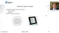
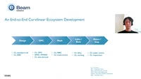
Presentation: Only Entirely Curvilinear Masks are Entirely Manufacturable Masks, Aki Fujimura, D2S [February 24, 2026]
>> View
Survey: 2026 Deep Learning/LLM Applications List by eBeam Initiative members [February 24, 2026]
>> View
Event: eBeam Initiative SPIE-AL Annual Lunch and Members Meeting, Tuesday, February 24, 2026
>> RSVP
Videos: Autumn 2025 Fine Line Video Journal [November 5, 2025]
>> View
Survey: 2025 eBeam Initiative Luminaries Survey Results [September 23, 2025]
>> View
Presentation: Technology Analysis of Leading-Edge Semiconductor Manufacturing, Tetsuya Wadaki, Morgan Stanley MUFG [September 23, 2025]
>> View
Press: eBeam Initiative Survey Predicts Continued Growth in Photomask Market This Year - AGC Joins eBeam Initiative [September 23, 2025]
>> English,
Japanese,
Simplified Chinese &
Traditional Chinese
Event: eBeam Initiative Reception during SPIE Photomask Technology + EUV Conference, Monterey, Calif.; 5:00–7:15pm Sept. 23, 2025
>> RSVP
Videos: Summer 2025 Fine Line Video Journal [June 3, 2025]
>> View
Presentation: Full-Reticle Curvilinear Inline Linearity Correction Including Variable Bias with Zero Turnaround Time by Paris Spinelli, Micron, at PMJ 2025 [April 18, 2025]
>> View
Presentation: Three Ways to Improve Wafer Uniformity by Aki Fujimura, D2S at PMJ 2025 [April 18, 2025]
>> View
Videos: Spring 2025 Fine Line Video Journal [March 26, 2025]
>> View
Presentation: PLDC Improves Uniformity and Linearity for All Masks by Aki Fujimura, D2S [February 25, 2025]
>> View
Event: Save the Date for the PMJ 2025 Finale hosted by the eBeam Initiative. Friday, April 18 right after the final session in the PMJ program and in the same room, the Annex Hall, Pacifico Yokohama.
>> RSVP
Press: eBeam Initiative Member Companies to Take Center Stage at SPIE Advanced Lithography and Patterning Conference [February 18, 2025]
>> View
Survey: 2025 Deep Learning Applications List by eBeam Initiative members [February 18, 2025]
>> View
Event:
eBeam Initiative SPIE-AL Annual Lunch and Members Meeting, Tuesday, February 25, 2025
Videos: Autumn 2024 Fine Line Video Journal [October 28, 2024]
>> View
Survey: 2024 eBeam Initiative Luminaries Survey Results [October 1, 2024]
>> View
>>View Features Archive
Mission | The Initiative provides a forum for educational and promotional activities regarding new design-to-manufacturing approaches based on electron beam (eBeam) technologies. The goals of the eBeam Initiative are to reduce the barriers to adoption to enable more IC design starts and faster time-to-market while increasing the investment in eBeam technologies.
Read the story of the eBeam Initiative
Design Team Advisors | Provide business and technical insights and requirements to the Steering Group and Ecosystem members.
eBeam Member Videos | Proof points, viewpoints and products discussed by eBeam Initiative members.

|
|
|

|
|
|

Semiconductor Engineering: Mask Economics Shape High-NA EUV Adoption [June 22, 2026]
>> View
Semiecosystem: Latest News in Lithography by Mark LaPedus [June 7, 2026]
>> View
Semiconductor Engineering: Curvilinear Masks Push the Limits of Inspection and Metrology [May 27, 2026]
>> View
Semiconductor Engineering: Mask Technology Faces a New Set of Challenges [May 21, 2026]
>> View
Semiconductor Engineering: eBeam Initiative at SPIE ALP 2026 [April 16, 2026]
>> View
Semiecosystem: Latest News in Lithography by Mark LaPedus [April 3, 2026]
>> View
Semiconductor Engineering: Challenges in Scaling Chips to 2nm and Below by Ed Sperling [March 30, 2026]
>> View
>>View News Archive